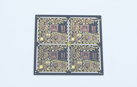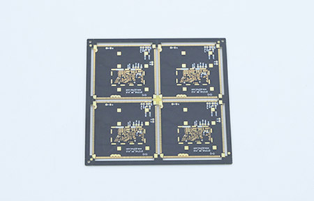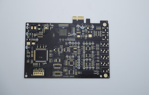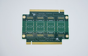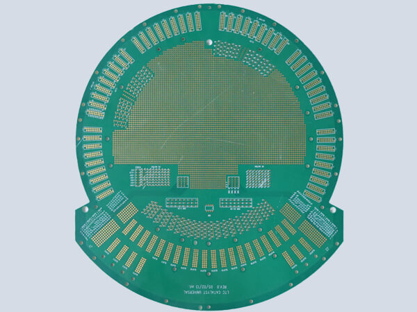
Through hole PCB
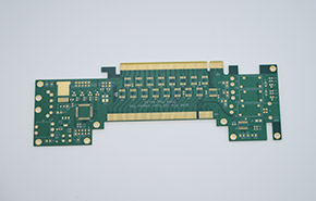
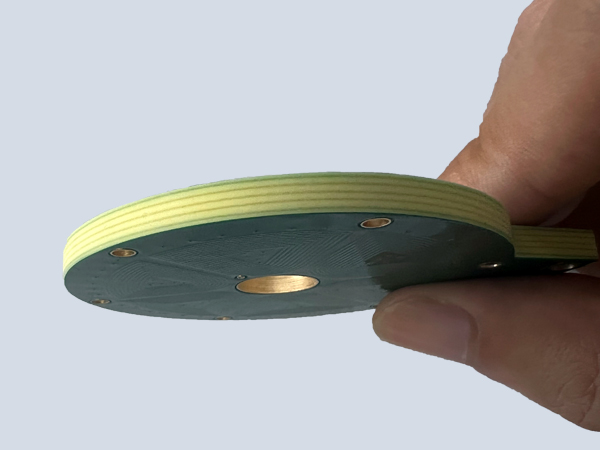
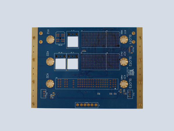
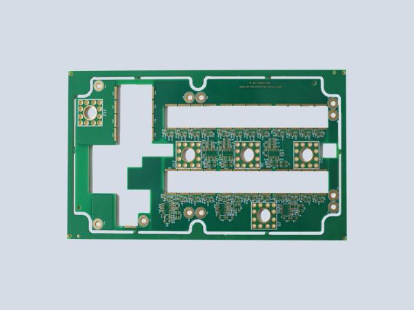
Layer number: 6 Material: Shengyi FR-4 Process: Sinking gold Minimum drilling hole: 0.3mm Copper thickness: 3oz Plate thickness: 2.5mm
Thick copper PCB is a layer of copper foil bonded onto a printed circuit board glass epoxy substrate. When the copper thickness is ≥ 2oz, it is defined as a thick copper plate ............
Phone:15361676619
Heavy copper PCB refers to a layer of copper foil bonded to a glass epoxy substrate on a printed circuit board (PCB) with a thickness of 2oz or greater. In PCB prototyping, heavy copper PCB requires a specialized process, requiring a certain level of technical expertise and operational complexity, and are relatively expensive.
Heavy copper PCB' performance: They carry high currents, reduce thermal strain, and dissipate heat well. They are not restricted by processing temperatures, allowing for oxygen-blast welding at high melting points and resisting brittleness at low temperatures. They are also fireproof and non-combustible. Even in corrosive environments, the copper forms a strong protective layer.
Heavy copper PCB is used in high-tech fields such as mobile phones, microwaves, aerospace, satellite communications, network base stations, hybrid integrated circuits, and high-power power supplies.
| material | Shengyi FR-4 | Number of layers | 6 |
| copper thickness | 1/2oz | Plate thickness | 2.5mm |
| Minimum aperture | 0.3mm | Surface Treatment | Metal edging+half hole |
