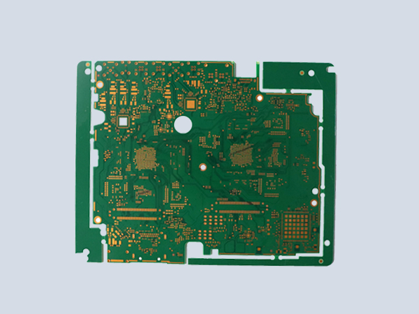
The stack-up structure is a key factor affecting the EMC performance of PCB and a crucial means of suppressing electromagnetic interference. With the continuous emergence of high-speed circuits, PCB is becoming increasingly complex. To prevent electrical interference, signal and power layers must be separated, leading to the design of HDI multi layer boards. So, what are the commonly used stack-up structures for HDI multi layer boards?
1. Simple Single-Buildup PCB
A single-buildup 6-layer board has a stack-up of (1+4+1). This type of board is the simplest, meaning the inner layers have no buried vias and can be laminated in a single step. Unlike multi layer boards, this type requires subsequent processes such as laser drilling of blind vias.
2. Conventional Single-Buildup HDI PCB
A single-buildup 6-layer HDI board has a stack-up structure of (1+4+1). This structure is (1+N+1), where N is an even number (N ≥ 2). This is the current mainstream design for single-build boards in the industry. The inner layers have buried vias, requiring a second lamination step.
3. Conventional Double-Layered HDI PCB
This 8-layer HDI double-layered board has a stacking structure of (1+1+4+1+1). This type of board has a structure of (1+1+N+1+1), where N ≥ 2, and N is an even number. This structure is the current mainstream design for double-layered boards in the industry. The inner layers have buried vias, requiring three press-fits.
4. The Second Conventional Double-Layered HDI PCB
This 8-layer HDI double-layered board has a stacking structure of (1+1+4+1+1). This type of board has a structure of (1+1+N+1+1), where N ≥ 2, and N is an even number. Although this is a double-layered board, the buried vias are located between layers (2-7) rather than between layers (3-6). This design reduces the number of press-fits, reducing the required three press-fits for double-layered HDI boards to a two-pass press-fit process.
5. Double-Layer HDI with Blind Via Stacking Design
Blind vias are stacked on top of buried vias in layers 2-7. This double-layer HDI 8-layer board has a stacking structure of (1+1+4+1+1). This board has a structure of (1+1+N+1+1), where N ≥ 2, and N is an even number. The inner multi layer board has buried vias and requires a second lamination.
6. Double-Layer HDI with Cross-Layer Blind Via Design
This double-layer HDI 8-layer board has a stacking structure of (1+1+4+1+1). This board has a structure of (1+1+N+1+1), where N ≥ 2, and N is an even number. This structure is currently a difficult double-layer board to manufacture in the industry. The inner multi layer board has buried vias in layers 3-6, requiring a third lamination.
7. Optimization of HDI Boards with Other Layer Structures
Triple-layer printed circuit boards (PCB) or PCB with more than three layers can also be optimized. A complete triple-layer HDI board requires four press-fits.