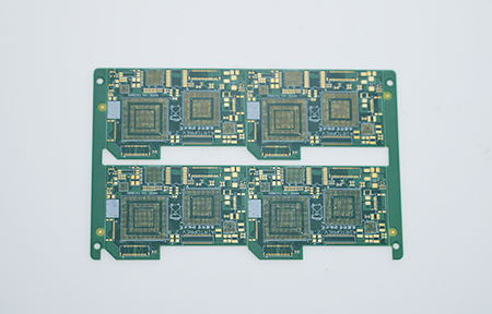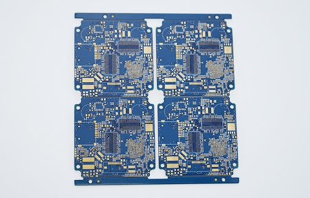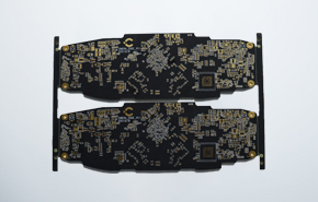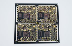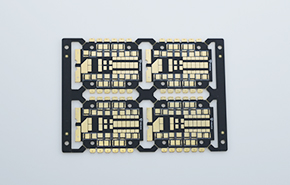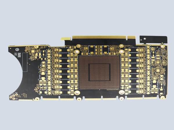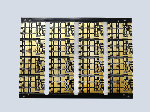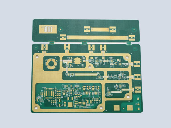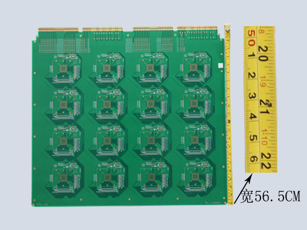
Multi-layer through hole PCB
Number of layers: 6; Material: FR4; Process: Immersion Gold; Min.drilling: 0.1mm; Min. trace width: 0.1mm; Min. trace spacing: 0.1mm
Phone:15361676619
Blind and buried via PCB, also known as HDI PCB, are often used in advanced products such as mobile phones, GPS navigation systems, and drone circuit boards. Conventional multi-layer PCB consist of inner and outer layers of circuitry, with connections between the layers achieved through drilling and in-hole metallization. As electronic products develop towards high density and high precision, PCB also need high precision and high density.
| material | FR-4 | Number of layers | 6 |
| copper thickness | 2oz | Plate thickness | 2.0mm |
| Minimum aperture | 0.1mm | Min. trace spacing | 0.1mm |
| Min. trace width | 0.1mm | Special process | second order |
