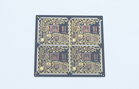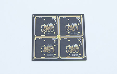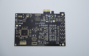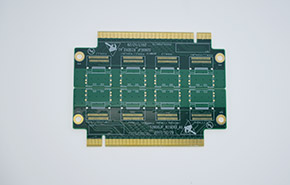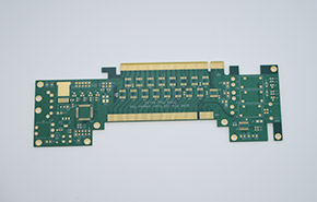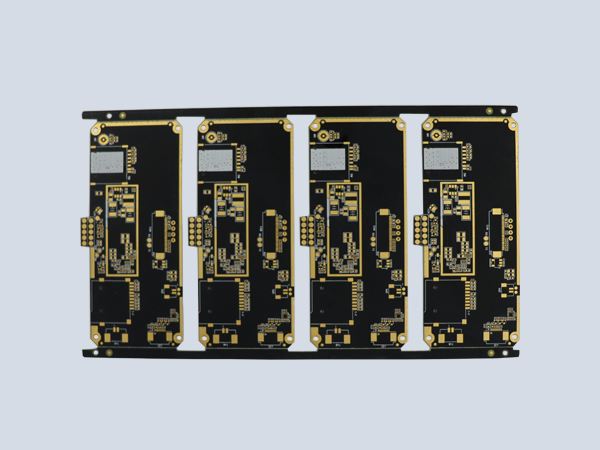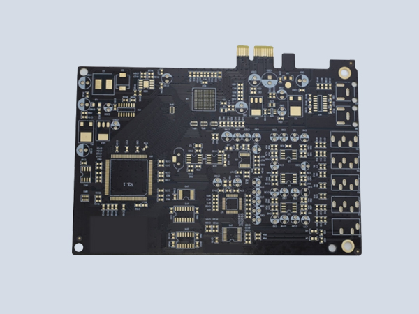
2-layer PCB for communication
Number of layers: 2 layers; Material: Teflon; Process: immersion gold; Min. drilling: 0.15mm; Min. trace width: 0.065mm; Min. trace spacing: 0.065mm
Phone:15361676619
Such PCB is simple structure and low cost. Designed for communication products with lower frequency requirements; not suitable for ultra-high-speed or high-frequency applications. Commonly used in low-cost wireless modules, simple sensor communication boards, and consumer electronics.
| material | ptfe | Number of layers | 2 |
| copper thickness | 1oz | Plate thickness | 1mm |
| Minimum aperture | 0.15mm | Min. trace spacing | 0.065mm |
| Min. trace width | 0.065mm | Surface Treatment | Immersion Gold |
