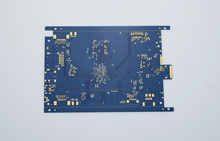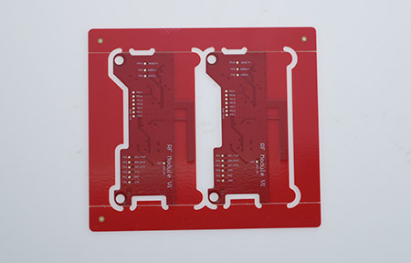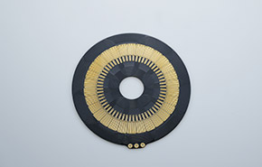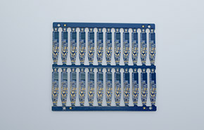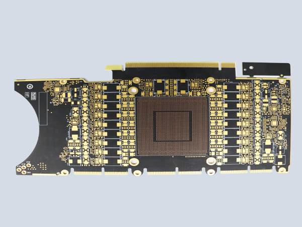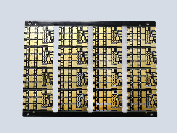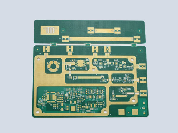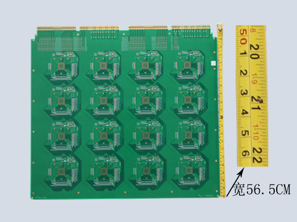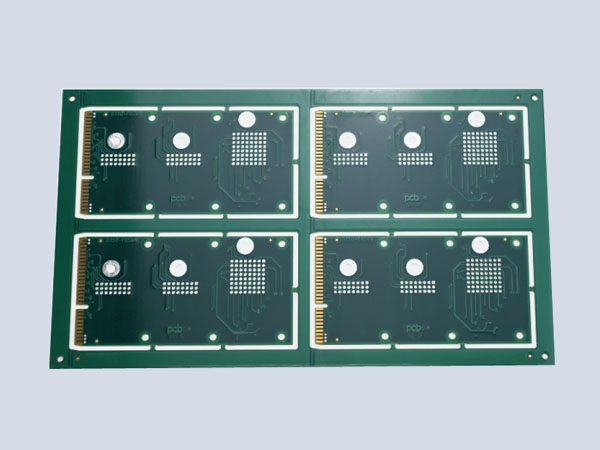
6-layer gold finger through hole PCB
Features: High thermal conductivity, fast heat dissipation. To ensure product quality, we start with raw materials and use A-grade military materials such as Shengyi/Jiantao and solar ink on the substrate .....
Phone:15361676619
Because the finger-like solder pads that connect to the metal springs in the card slots require high surface wear resistance and conductivity, they are plated with a layer of nickel and gold, commonly known as gold fingers.
The contact and conduction between the gold fingers and the springs in the card slots allows interconnection between the external PCB and the motherboard, while also facilitating easy removal and replacement based on user performance requirements.
Gold Finger PCB Features:
1. Low contact resistance, strong wear and corrosion resistance;
2. Regular, long, short, and segmented gold fingers;
3. Suitable for memory modules, solid-state drives, graphics cards, etc.
| material | TU872SLK | Number of layers | 6 |
| copper thickness | 1oz | Plate thickness | 1.6mm |
| Minimum aperture | 0.15mm | Min. trace spacing | 0.075mm |
| Min. trace width | 0.065mm | Surface Treatment | Immersion Gold |
