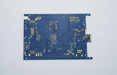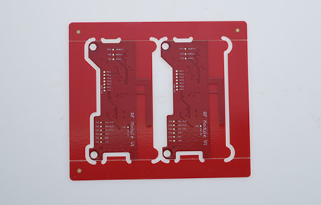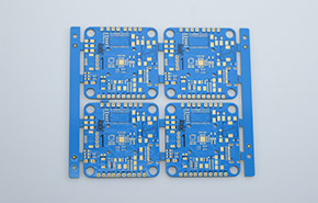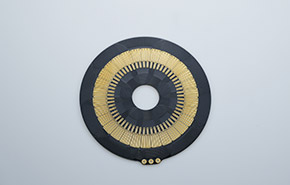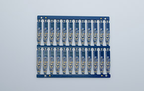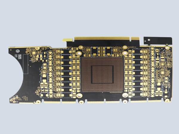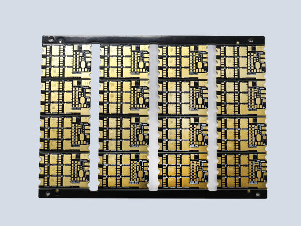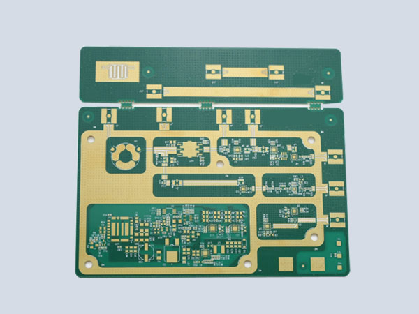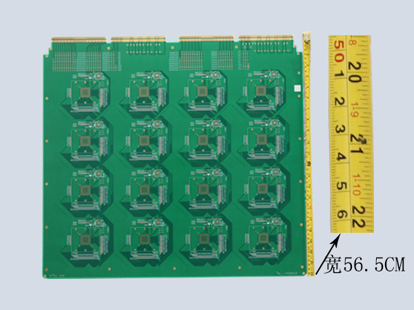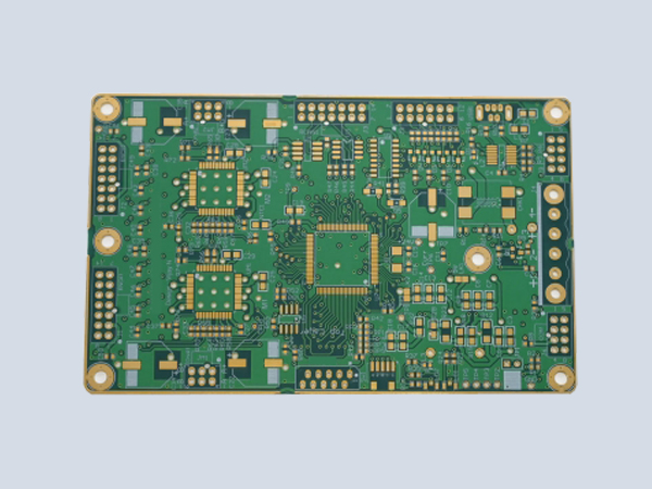
Multi-layer through hole PCB
Advantages of multi-layer PCB board: high assembly density, small size, and light weight. Due to the high assembly density, the number of connections between components (including electronic components) is reduced, thus improving reliability;
Phone:15361676619
Multi-layer PCB advantages: high assembly density, small size, light weight. Due to the high assembly density, the connection between components is reduced, thereby improving reliability; the number of wiring layers can be increased, thereby increasing design flexibility; it can form a circuit with a certain impedance; it can form a high-speed transmission circuit; circuit and magnetic circuit shielding layers can be set, and a metal core heat dissipation layer can be set to meet the needs of special functions such as shielding and heat dissipation; simple installation and high reliability.
| material | Shengyi S1141 | Number of layers | 6 |
| copper thickness | 1oz | Plate thickness | 1.6mm |
| Minimum aperture | 0.2mm | Min. trace spacing | 0.075mm |
| Min. trace width | 0.075mm | Surface Treatment | Sinking gold+metal edging |
