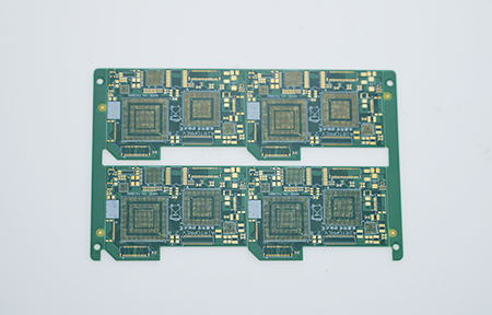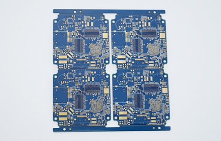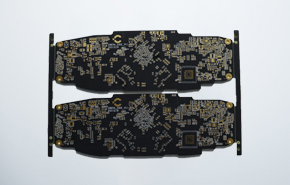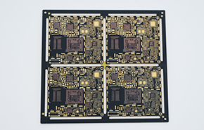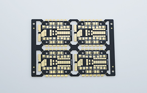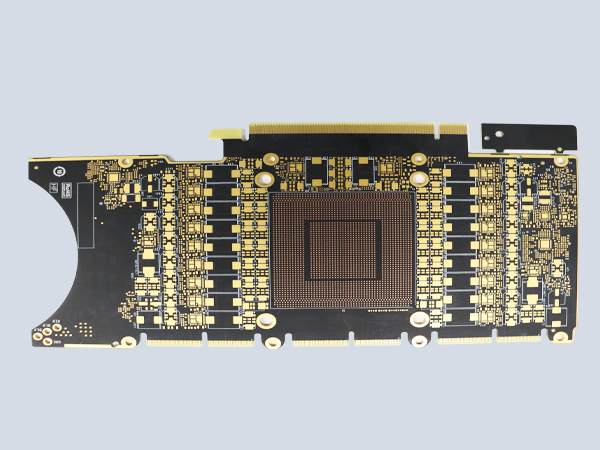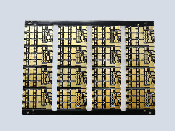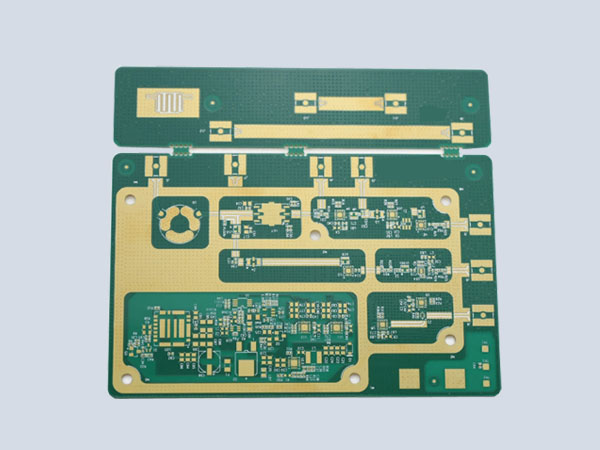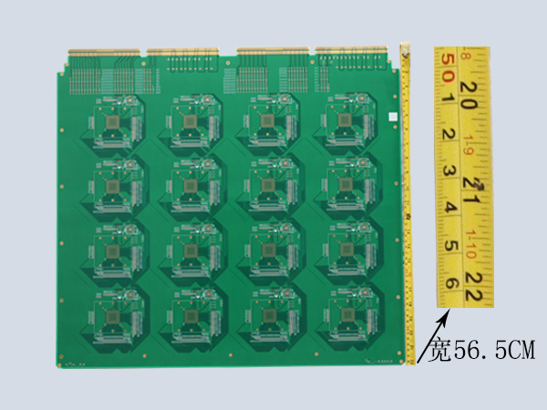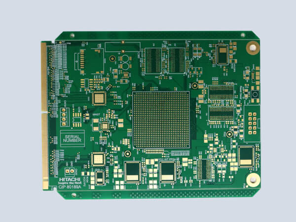
Multi-layer through hole PCB
The use of gold plating on the gold finger PCB HDI circuit board actually refers to thick gold, hard gold, also known as plug gold plating, rather than the whole board gold plating, soft board. The characteristic of this type of gold is that it is relatively hard, can be plated very thick, and resistant to insertion and extraction ....
Phone:15361676619
Because the finger-like solder pads that connect to the metal springs in the card slots require high surface wear resistance and conductivity, they are plated with a layer of nickel and gold, commonly known as gold fingers.
The contact and conduction between the gold fingers and the springs in the card slots allows interconnection between the external PCB and the motherboard, while also facilitating easy removal and replacement based on user performance requirements.
Gold-finger circuit boards are typically thick, hard gold, also known as plug gold plating, and do not refer to full-board gold plating or flexible circuit boards. This type of gold is characterized by its hardness, allowing for very thick plating and durability. Often, the term "gold-finger card boards" refers to this type of board.
Hard gold offers greater wear resistance and can withstand 20,000 plug-in and pull-out cycles without affecting quality. It requires a thickness of at least 5U. However, hard gold processing is relatively complex, and the high thickness required consumes more gold salts, leading to high costs.
It is often used in devices that require frequent plugging and unplugging, such as graphics cards, memory modules, expansion cards, and communication device interfaces.
| material | FR-4 | Number of layers | 16 |
| copper thickness | 1oz | Plate thickness | 2.0mm |
| Minimum aperture | 0.15mm | Min. trace spacing | 0.075mm |
| Min. trace width | 0.075mm | Surface Treatment | Sinking Gold+Golden Fingers |
