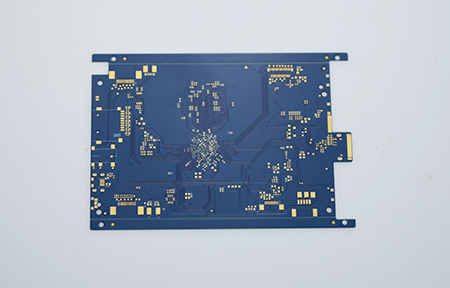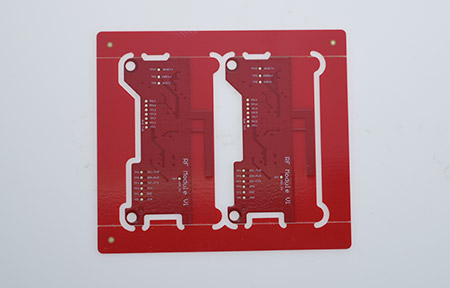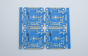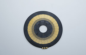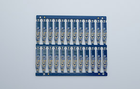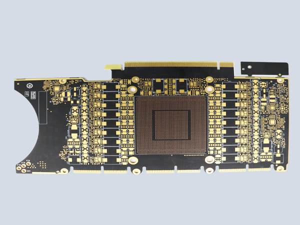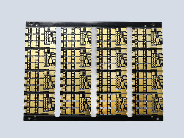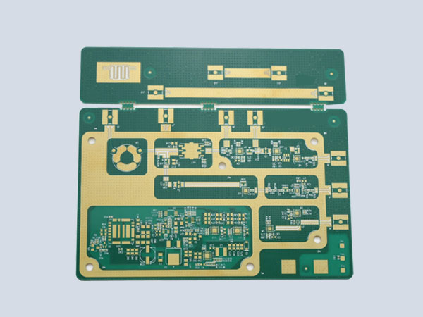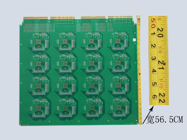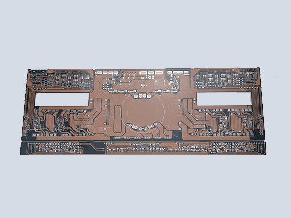
Multi-layer through hole PCB
Number of layers: 6 layers; Material: F4BM-300; Process: Immersion Gold; Min. drilling: 0.15mm; Min. trace width: 0.065mm; Min.trace spacing: 0.065mm
Phone:15361676619
A simple way to visually identify a through-hole PCB is to hold it up to a light. Any hole that glows is a "through hole." You can also think of it as a hole that can pass a wire.
Through holes are the most common holes in PCB, primarily providing electrical connections. Traditionally, through holes are categorized as either plated or non-plated. This is manufacturing terminology; in design, holes are categorized as either solderable or non-solderable.
PCB manufacturers have their own set of standard hole sizes to choose from when drilling holes, but they can generally use any standard hole size. Generally, PCB manufacturers can produce through-hole diameters smaller than 0.15 mm, with a typical size of 0.6 mm.
| material | F4BM-300 | Number of layers | 6 |
| copper thickness | 1oz | Plate thickness | 1.6mm |
| Minimum aperture | 0.15mm | Min. trace spacing | 0.065mm |
| Min. trace width | 0.065mm | Surface Treatment | Immersion Gold |
