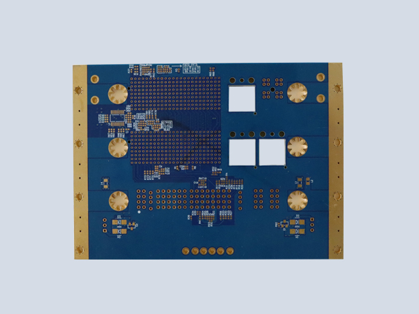
In the pattern electroplating method of multi-layer circuit board manufacturers, the power circuit pattern is prone to side corrosion during the entire etching process, resulting in a suspension layer of tin lead alloy plating that is suspended in the air and easily falls off, causing short circuit faults in the middle of the transmission line due to bridging mode. The multi-layer circuit board factory uses infrared hot melt technology to maintain the exposed copper surface better. However, when used for infrared thermal melting of multi-layer circuit boards, the extremely high ambient temperature causes severe layer by layer bubbling between the layers, resulting in a very low output rate of multi-layer circuit boards. What are the reasons for the quality problems of multi-layered circuit boards with layered bubbles?

Cause: (1) To prevent unreasonable accumulation of gases, water vapor, and pollutants, solution: Within multi-layer circuit board manufacturers, multi-layer boards need to be baked and kept clean before stacking; Strictly control the pre - and post process procedures to ensure that the processing environment and process indicators meet technical standards. (2) In the prevention process, due to insufficient heat generation, short cycle time, poor quality of the semi cured film, incorrect operation of the press, and even problems with the drying and solidification level. Solution: Check the Tg of the solid wood multi-layer board that has been stopped, or check the temperature record of the stopping process to stop the processing of the semi-finished product. The multi-layer circuit board manufacturer will then re bake it at 140 ℃ for 2-6 hours for smooth curing treatment. (3) When the blackening treatment of the inner layer is poor or the surface is damaged due to deterioration, the solution is for multi-layer circuit board manufacturers to strictly control the process indicators of the oxidation tank and cleaning tank on the deterioration production line, and improve the appearance quality of the detection surface by using double-sided treated copper paste. (4) Internal multi-layer board or semi cured sheet contamination, solution: the cleaning and management methods in the work area and storage area need to be improved; Reduce the frequency of manual transportation and continuous board retrieval; Various loose materials should be covered to prevent environmental pollution during stacked operation; When the special tool nut must undergo surface treatment for lubrication and denitrification, it must be separated from the stacked work area and cannot be carried out in the stacked work area. (5) The total flow rate of the adhesive is insufficient. Solution: The multi-layer circuit board manufacturer should moderately increase the pressure strength of the compression; Moderately alleviate the heating rate and increase the duration of glue flow, or use more kraft paper bags to alleviate the heating curve; Dismantle and replace semi cured sheets with high amount of adhesive or long curing time; Check whether the surface of the thick steel plate is flat and flawless; Check if the length of the snap spring is too long, causing the heating plate to not be tightly attached and resulting in insufficient heat transfer process; Check if the compressed air system of the vacuum pump multi-layer press is excellent. (6) Excessive glue flow - within the range of the amount of glue used in the semi cured film, squeeze the board outside. Solution: multi-layer circuit board manufacturers should adjust or reduce the working pressure used in a timely manner; The front inner multi-layer board needs to be baked to remove moisture, as moisture will expand and accelerate the flow of glue; Change to a semi cured sheet with a relatively low flow rate or short gelation time. (7) In the case of ineffective use, the inner multi-layer board should try to avoid the formation of large copper surfaces (as the bonding between epoxy resin and copper surface is much lower than that between epoxy resin and resin). Solution: Multilayer circuit board manufacturers should etch away meaningless copper surfaces as much as possible.