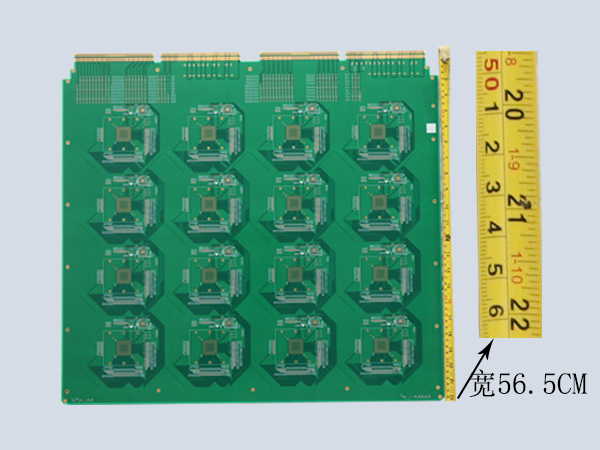
Via is one of the important components of multi-layer PCB, and the cost of drilling holes usually accounts for 30% to 40% of the PCB manufacturing cost. From a design perspective, a via mainly consists of two parts: a drill hole in the middle and a pad area around the drill hole. The size of these two parts determines the size of the via. Obviously, in high-speed and high-density PCB design, designers always hope that the smaller the via, the better, so that there can be more wiring space on the board. In addition, the smaller the via, the smaller its own parasitic capacitance, making it more suitable for high-speed circuits. However, the reduction in hole size also brings about an increase in cost, and the size of through holes cannot be reduced without restrictions. It is limited by processes such as drilling and plating: the smaller the hole, the longer it takes to drill and the easier it is to deviate from the center position; And when the depth of the hole exceeds 6 times the diameter of the borehole, it cannot be guaranteed that the hole wall can be uniformly plated with copper.

1. Through holes are a part of printed circuit board (PCB) design, and their function is to connect, fix, and position electrical components. A via consists of three parts: the hole, the pad area around the hole, and the POWER layer isolation area. The production of through holes: A layer of metal is plated on the cylindrical surface of the hole wall of the through hole to connect the copper foils in the middle layers. The upper and lower sides of the through hole are made into solder pads for direct circuit connection (or not). 2. Through holes are generally divided into three categories: blind holes, buried holes, and through holes. Blind hole - located on the top and bottom surfaces of a printed circuit board, with a certain depth (hole diameter and hole depth in a certain ratio), used for connecting surface and inner layer circuits. Buried hole - a connection hole in the inner layer of the circuit board (not visible on the surface of the circuit board). Through hole - passes through the entire circuit board and is generally used for component positioning and installation. 3. In general PCB design, due to the small impact of parasitic capacitance and inductance of vias, vias with a diameter of 0.36mm (aperture)/0.61mm (pad)/1.02mm (POWER isolation area) are usually selected for the via design of PCBs on layers 1 to 4. For signal lines with special requirements, such as power lines, ground lines, etc., 0.41mm/0.81mm/1.32mm vias are generally used.