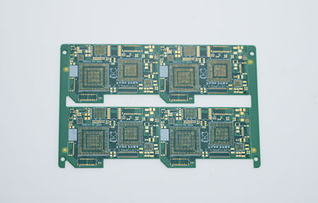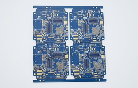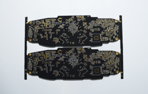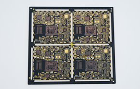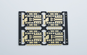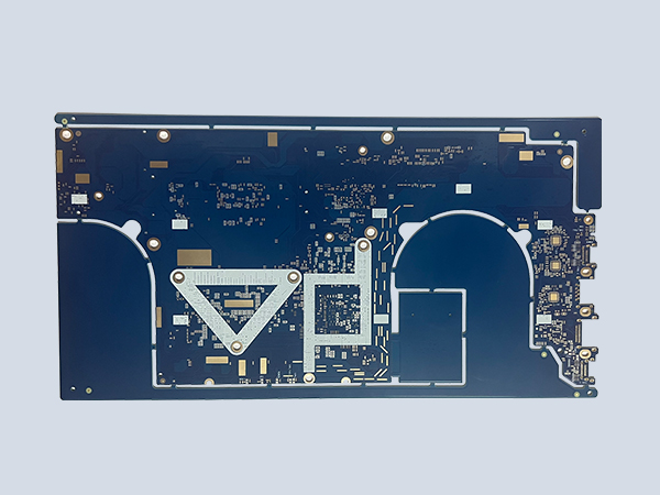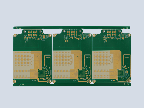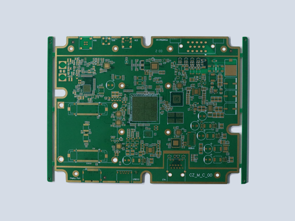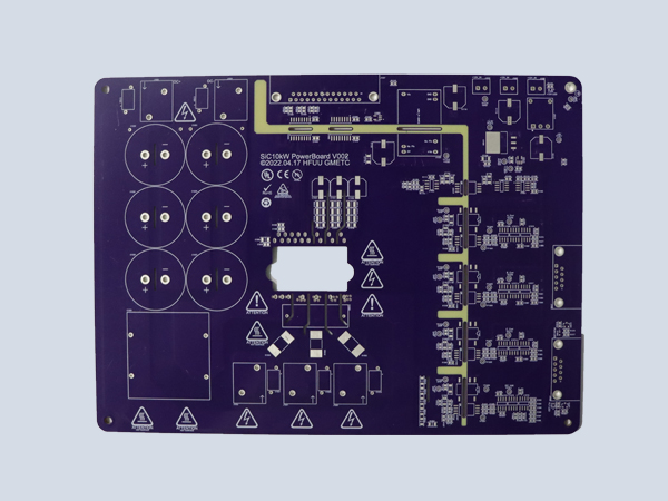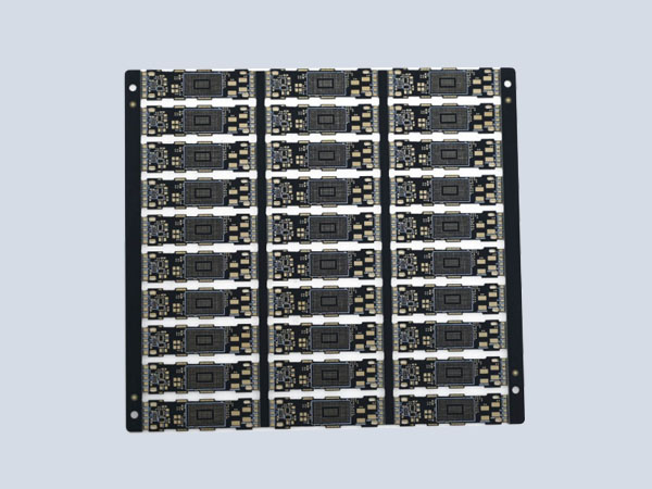
6-layer 2nd order HDI PCB
HDI circuit boards are compact products designed specifically for small capacity users. We can customize PCB boards with various high difficulty and complex processes according to your requirements .....
Phone:15361676619
HDI is an abbreviation for High Density Interconnect. It is a type of printed circuit board (PCB) technology that uses micro-blind buried vias to achieve a relatively high trace density. HDI is a compact product designed for low-volume users.
Blind vias: These are vias that connect traces on inner layers of a PCB to traces on the surface without penetrating the entire board. (Generally used on PCB with four or more layers.)
Buried vias: Buried vias connect traces only between inner layers and are invisible from the PCB surface. (Generally used on PCB with six or more layers.)
Advantages: They increase trace spacing.
Disadvantages: The process is costly and is not commonly used in electronic products, except for very advanced products.
| material | FR-4 | Number of layers | 10 |
| copper thickness | 1oz | Plate thickness | 1.6mm |
| Minimum aperture | 0.1mm | Min. trace spacing | 0.065mm |
| Min. trace width | 0.065mm | Surface Treatment | Immersion Gold |
