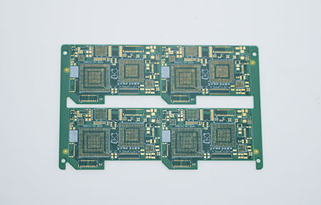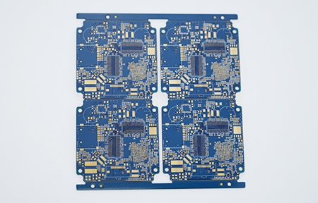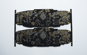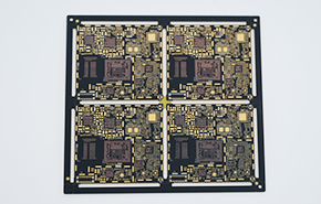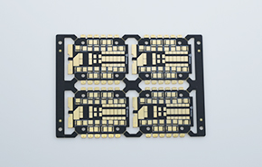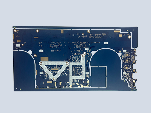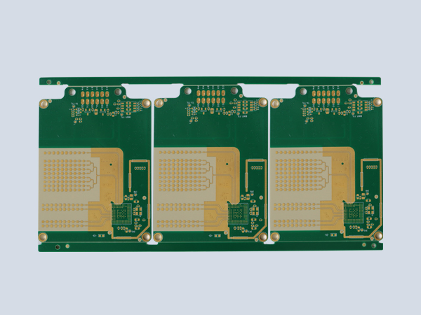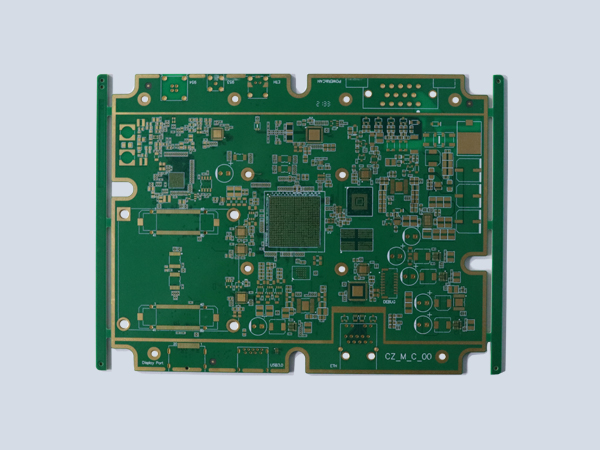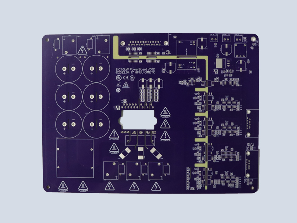
Blind & buried vias PCB
HDI is an abbreviation for High Density Interconnector, which is a technology used in the production of printed circuit boards. It is a type of circuit board that uses micro blind buried hole technology to achieve a relatively high distribution density of circuits.
Phone:15361676619
HDI is an abbreviation for High Density Interconnect. It is a type of printed circuit board (PCB) technology that uses micro-blind buried vias to achieve a relatively high trace density. HDI is a compact product designed for low-volume users.
Blind vias: These are vias that connect traces on inner layers of a PCB to traces on the surface without penetrating the entire board. (Generally used on PCB with four or more layers.)
Buried vias: Buried vias connect traces only between inner layers and are invisible from the PCB surface. (Generally used on PCB with six or more layers.)
Advantages: They increase trace spacing.
Disadvantages: The process is costly and is not commonly used in electronic products, except for very advanced products.
